DE1-SoC IDE Verilog
Program Altera FPGA DE1-SoC in Verilog

LabsLand FPGA Community
Learn Hardware design with FPGAs using DE1-SoC
Laboratory information
Learn Hardware design with FPGAs using Terasic DE1-SoC!
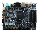
In this laboratory, you can learn how to program using two Hardware Design Languages: VHDL or Verilog, and test your code in a real Terasic DE1-SoC FPGA. The FPGA has a set of components already place, such as 10 red LEDs, 6 7-segment displays or multiple clocks. In addition, you will have access to 10 virtual switches and 4 virtual buttons that you can use in your design and that you will see when interacting with the real hardware. This way, you will be able to turn on and off the switches or press the buttons and see how your design behaves. The boards are located in different universities, as you will see when using each board.
In this laboratory, you do not need any software or hardware installed in your computer, tablet or phone.
What students do
Video
Available experiments
Program Altera FPGA DE1-SoC in Verilog
Program Altera DE1-SoC DE1 in VHDL
Program Altera FPGA DE1-SoC in SystemVerilog
Teaching resources
How to adapt external VHDL or Verilog codes or external practices to the LabsLand FPGA laboratory
Open resourceIntroduction to the LabsLand FPGA laboratory. Activity that involves the design of a combinational ALU that makes simple arithmetical operations.
Through this activity the following goals will be met:
Use the breadboard to map GPIO to switches and LED's
Open resource80+ pages of contents on how to use the FPGA laboratory, Boole Designer, Digital Trainer
Open resourceIntroduction to the LabsLand FPGA laboratory. Activity that involves the design of a combinational ALU that makes simple arithmetical operations.
(This is the solved version of this practice. The not-solved version is a different version of this practice).
Through this activity the following goals will be met: