License LCAL0001
Intel FPGA Laboratories
Remote access to 8 laboratories included:
The equipment is always real, not a simulation. Access now. No need to wait for an equipment to be shipped.
Laboratories included in this license
 Boole Designer
 Digital Trainer
 FPGA Laboratory
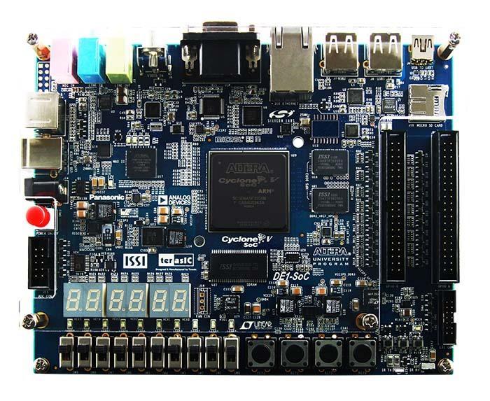 DE1-SoC
- DE1-SoC (binary upload)
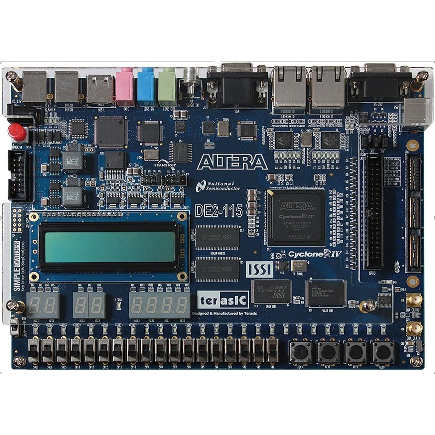 Altera DE2-115
- Intel DE2-115 (no IDE)
- DE1-SoC · Nios V
How does LabsLand work?
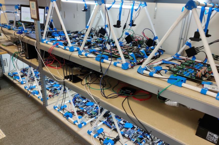
LabsLand is a global network of real laboratories available online. Students (in schools, universities and life-long learning platforms) can access the real laboratories through the Internet, using their laptop, tablet or phone.
In every case, the laboratory is always real (not simulated), and available through the Web (you do not need to obtain any hardware, deal with shipping, etc.).
Bulk licenses
If you are going to buy multiple licenses (e.g., for a classroom or group of users, or institutional license), contact us for discounts.
You buy LabsLand licenses as an individual in the links below, or for your institution. If you buy licenses for your institution, you have to reach out so we can provide you with a space for your institution where you can keep track of the usage by users and obtain other institution-focused tools.
Boole Designer
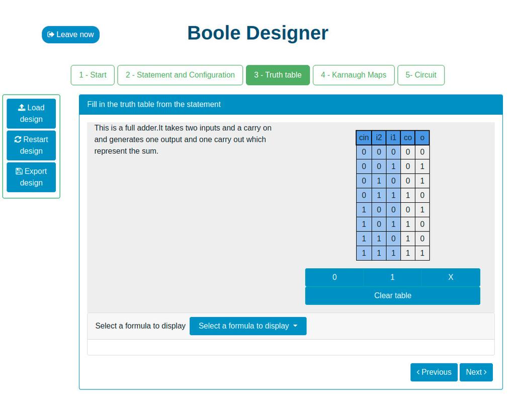
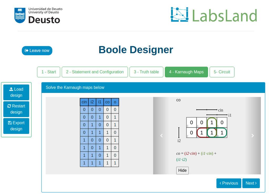
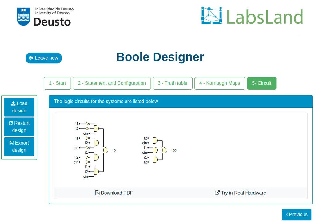
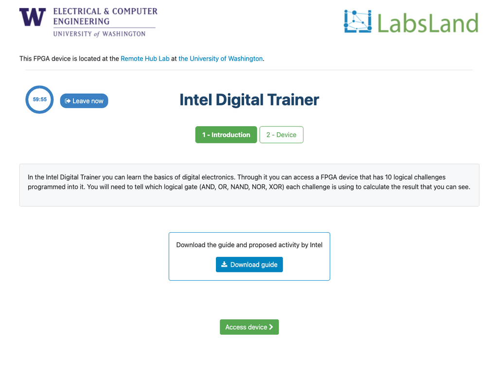
This laboratory will let you learn basic Digital Electronics.
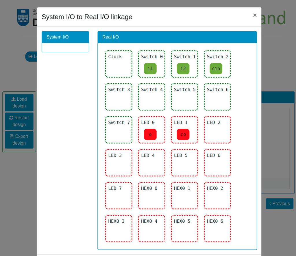
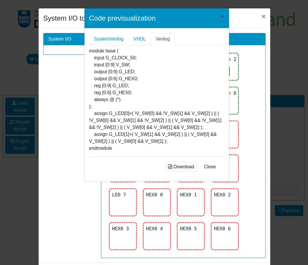
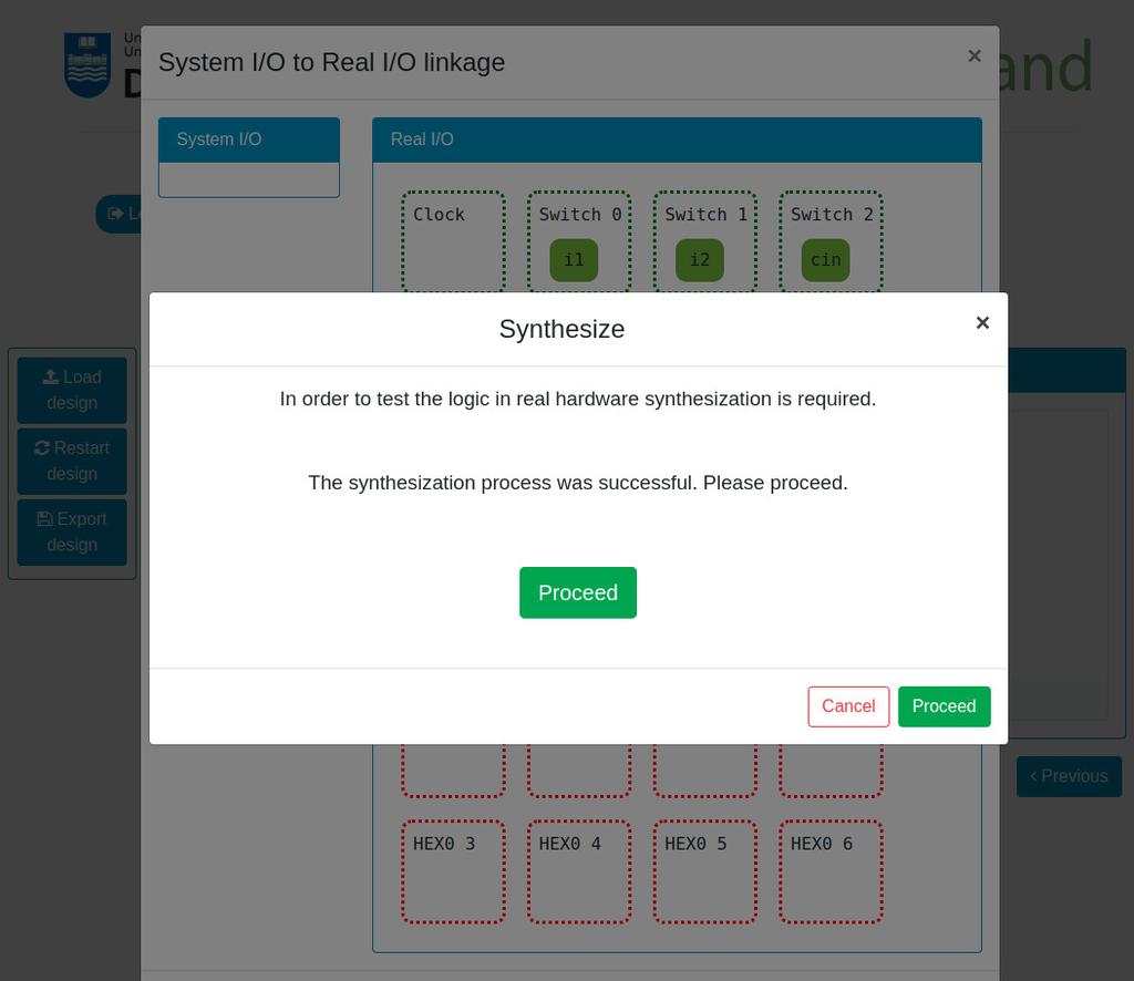
You will be able to design Combinational Systems by designing and filling a truth table, use Boolean Algebra, create Karnaugh–Veitch (KV or VK) maps, and try the systems that you create in real remote hardware (Intel FPGAs).

Digital Trainer
Summary
The Digital Trainer laboratory is designed towards students that are starting with digital logic, truth tables and Boole's Algebra.
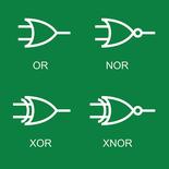
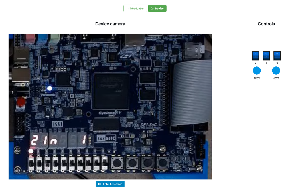
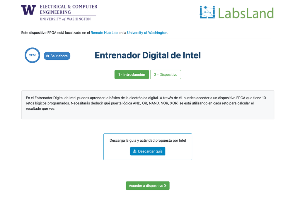
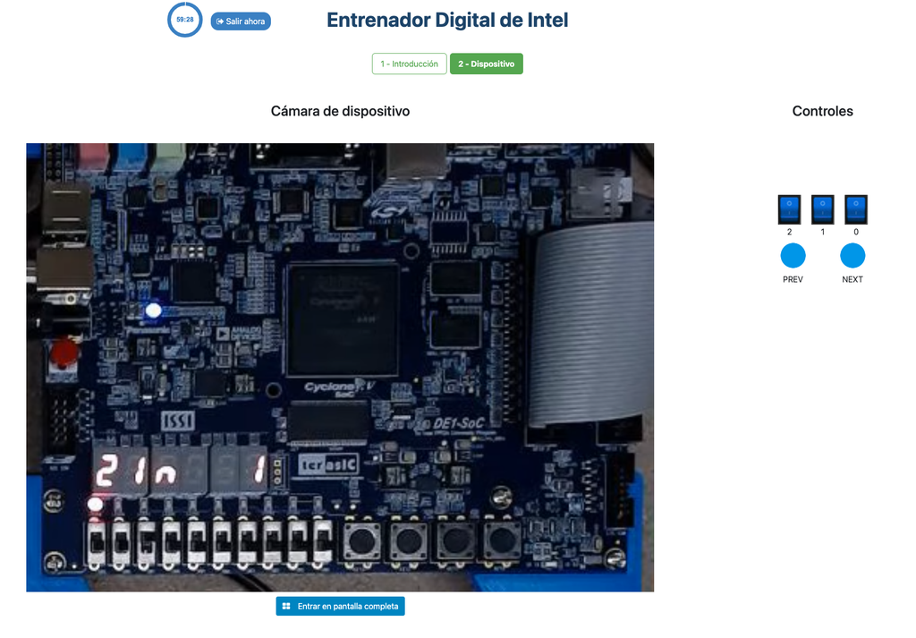
During the activity, the student sees an Intel FPGA that implements a series of simple truth tables. The student can interact with the FPGA devices to vary the inputs to the system through switches, and observe the outputs through LEDs. The challenge is to determine which logical operator the FPGA implements in each case (e.g. AND, NAND...).
Further details
The activity is designed to be relatively simple and straightforward, but at the same time to be engaging for the students. It is designed in a game-like style, and it is based in real hardware (FPGAs). That way, it is not only useful to introduce and obtain familiarity with digital logic, but also it allows students to start seeing the future uses of that knowledge, interacting in a superficial way with FPGA devices, of the same kind that are used in industry.
Interaction with the FPGA devices does not add complexity, since students don't need to program them; they already implement a black box logic (which is precisely the point of the activity).
The laboratory is originally based in an activity that Intel Corporation frequently conducts in its seminars, both hands-on and remote, using their Intel DE1-SoC, Intel DE2-115, or other types of FPGAs.
FPGA Laboratory
Learn Hardware design with real FPGAs!
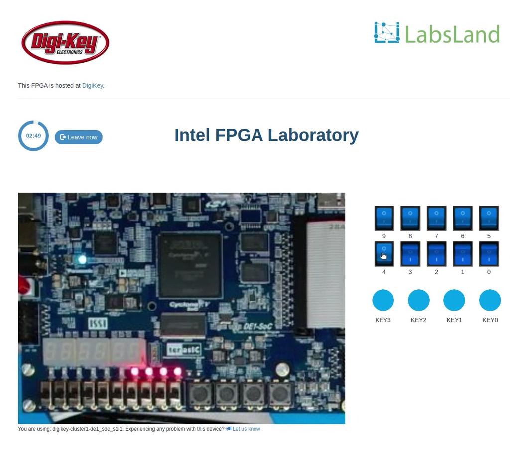
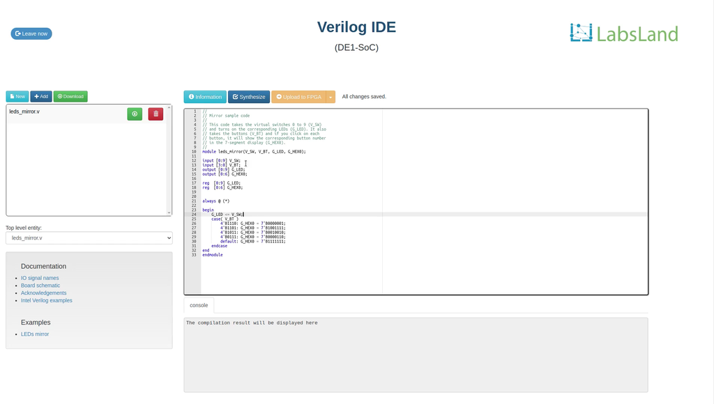
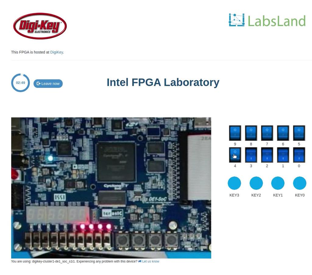
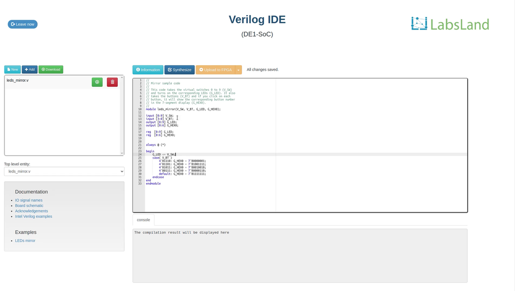
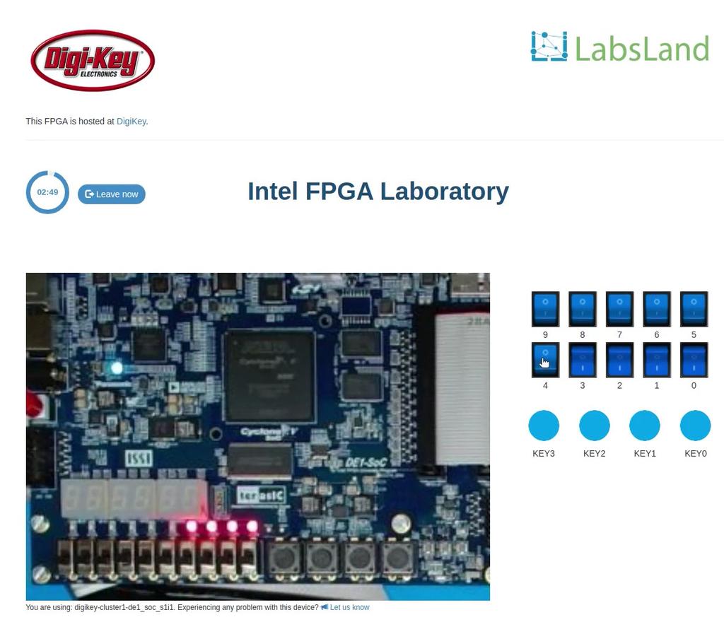
In this laboratory, you can learn how to program using two Hardware Design Languages: VHDL or Verilog, and test your code in one of our multiple boards available. Every FPGA has a set of components already place, such as 10 LEDs, 6 7-segment displays or multiple clocks. In addition, you will have access to 10 virtual switches and 4 virtual buttons that you can use in your design and that you will see when interacting with the real hardware.
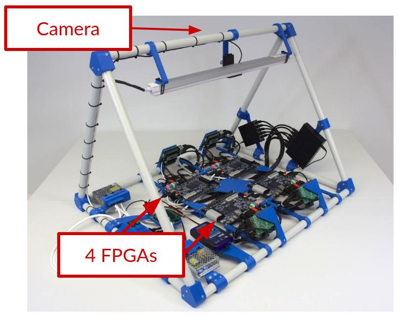
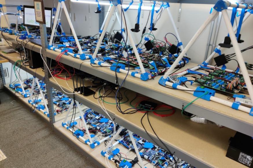
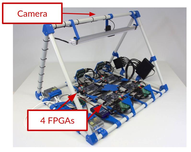
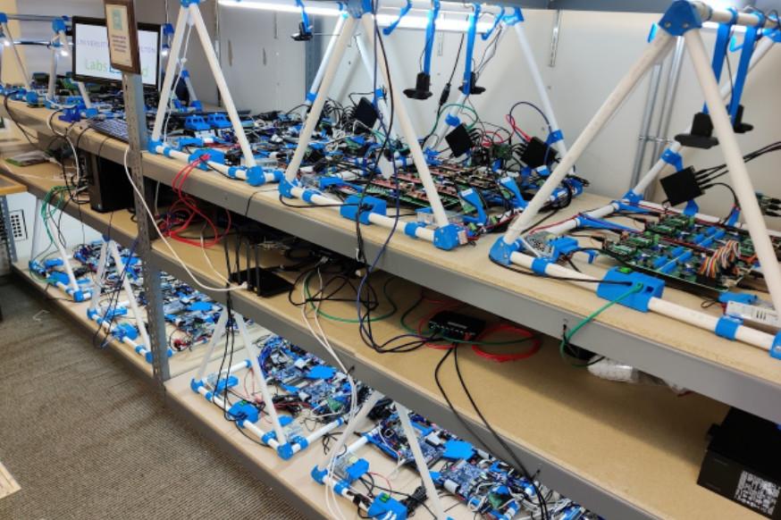
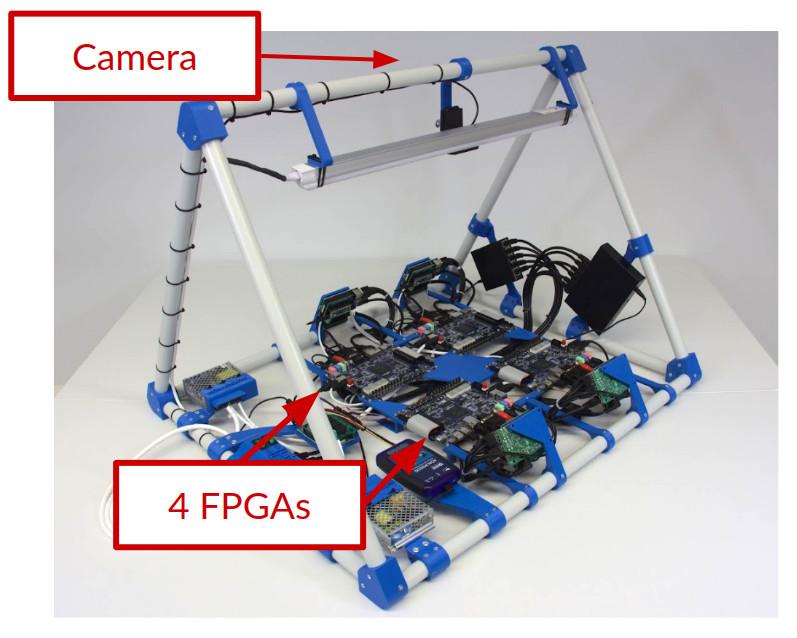
Whenever you synthesize your code, you will be assigned to a particular board (such as Terasic DE2-115 or Terasic DE1-SoC or others), and you will be able to send your code to one of the available boards and to turn on and off the switches or press the buttons and see how your design behaves. The boards are located in different universities, as you will see when using each board.
In this laboratory, you do not need any software or hardware installed in your computer, tablet or phone.
DE1-SoC
Write and compile your design in the browser, then test it on a real DE1-SoC. Observe the LEDs and seven-segment displays through the live camera and interact using the virtual switches and buttons.
To use UART, choose Standard in the interface selector and enable the UART serial terminal before entering. UART sessions use compatible boards.
DE1-SoC (binary upload)
Create and compile your FPGA design in Quartus, then upload the .sof file here. Choose the standard interface for direct access, or select an interface before entering to use other available controls and simulations.
To use UART, choose Standard in the interface selector and enable the UART serial terminal before entering. UART sessions use compatible boards.
Intel DE2-115 (no IDE)
Learn Hardware design with FPGAs using Terasic DE2-115!
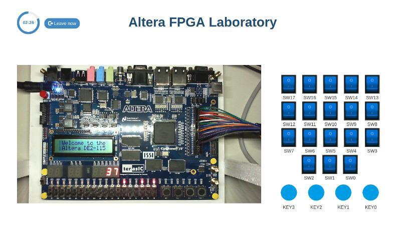
In this laboratory, you can learn how to program using two Hardware Design Languages: VHDL or Verilog, and test your code in a real Terasic DE2-115 FPGA. The FPGA has a set of components already place, such as LEDs, 7-segment displays or multiple clocks. In addition, you will have access to 18 virtual switches and 4 virtual buttons that you can use in your design and that you will see when interacting with the real hardware. This way, you will be able to turn on and off the switches or press the buttons and see how your design behaves. The boards are located in different universities, as you will see when using each board.
In this laboratory, you do not need any software or hardware installed in your computer, tablet or phone.